
Semiconductor Wafer Inspection: Measurement Solutions from Nanometer Precision to Full-Size Coverage
Posted2026-7-8

Precision measurement solutions for wafer flatness and critical dimensions in the semiconductor industry
Competition in semiconductor manufacturing is fundamentally a race for precision. As process nodes advance to 7nm, 5nm, and beyond, even the slightest deviation in every circuit line or alignment mark on a wafer directly impacts final chip yield. For wafer manufacturers, inspection is not merely the "final checkpoint" of quality control; it is a core control point embedded throughout the entire manufacturing process.
Three Challenges in Wafer Inspection
The difficulty of semiconductor wafer inspection stems from the convergence of three dimensions.
First is the scale span. On a single 300mm wafer, you must assess both overall flatness—which affects depth-of-focus consistency and warpage control during lithography—and microscopic parameters such as line width and overlay accuracy. The scale difference between these two spans several orders of magnitude, making it difficult for a single inspection tool to cover both macroscopic topography and microscopic features.
Second is efficiency pressure. Advanced process wafer lines are scheduled in hour-long intervals; if inspection cannot match the production cycle, it becomes a bottleneck for the entire line. Traditional contact measurement or point-by-point scanning struggles to balance speed and accuracy when handling high-volume online inspection demands.
Third is data integrity. Semiconductor manufacturing demands extremely strict quality traceability—every wafer and every batch of inspection data must be fully retained to quickly pinpoint the source of yield anomalies. If an inspection system only outputs results without recording process data, it cannot meet the traceability requirements of modern fabs.
Macro-to-Micro Synergy: One Solution for Full-Scale Inspection
To address these challenges, Makai Intelligent Measurement proposed a full-scale inspection solution combining the Versa-F flagship optical profiler with a white light interferometer. The core of this approach integrates macroscopic profile measurement and microscopic feature analysis into a single workflow, minimizing errors caused by equipment switching and sample handling.
In the wafer flatness inspection stage, white light interferometry plays a key role. As a non-contact surface topography measurement technique based on optical interference, it achieves sub-nanometer vertical resolution. It captures full-wafer flatness data, roughness distribution, and warp without contacting the wafer surface, providing critical input for adjusting lithography process parameters.
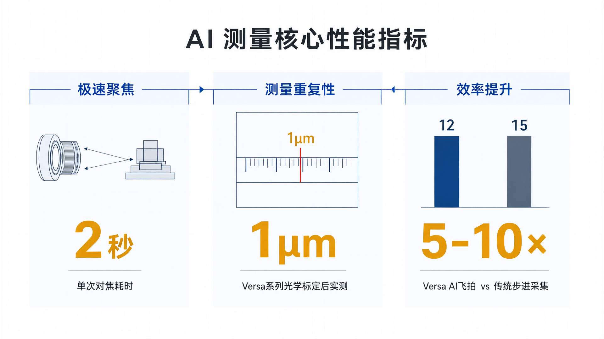
During critical dimension (CD) measurement, the Versa-F flagship vision system leverages AI Fly-Scan technology. Developed in-house by Maike Intelligent Measurement, this high-speed imaging and intelligent recognition solution uses deep learning algorithms to analyze captured images in real time, enabling measurements of line width, pitch, and overlay accuracy while the stage is in motion. Compared to traditional stop-and-scan methods, Fly-Scan boosts single-wafer measurement efficiency by several times without compromising accuracy.
In the defect detection phase, Versa-F's high-resolution optical system works in tandem with MicroCore AI-powered metrology software. MicroCore is the core software platform of Maike Zhice, integrating image preprocessing, defect recognition, dimensional measurement, and data management. It automatically identifies anomalies on the wafer surface—such as scratches, particles, and pattern defects—and outputs structured data including defect location, type, and size for direct integration into the fab's quality management system.
Data-Driven Results: Quantified Gains in Efficiency and Yield
The effectiveness of this solution in real-world applications can be quantified across three dimensions.
AI-powered automatic imaging significantly reduces online inspection time per wafer, boosting overall inspection efficiency by approximately 5x. This means a single system can now handle tasks that previously required multiple devices to rotate, directly reducing equipment investment and production floor footprint.
Yield improvements are driven by full-coverage inspection that significantly boosts defect detection. Macro-level flatness anomalies and micro-scale dimensional deviations are correlated within a single data pipeline, enabling process engineers to precisely identify root causes—whether from focus depth shifts in lithography, uneven etch rates, or abnormal thin-film stress. This accurate attribution has increased product yield by approximately 30%.
For quality traceability, MicroCore automatically records complete raw images, measurement parameters, and environmental data for every inspection, creating a fully auditable test archive. When anomalies are detected during packaging and testing, engineers can quickly trace back to the corresponding wafer-level inspection data within minutes to pinpoint the root cause.
From Detection to Decision: Unlocking the Full Value of Measurement Data
The value of full-scale inspection goes beyond "finding defects." When flatness, critical dimensions, and defect distribution data converge on a single platform, they form a digital twin of the wafer manufacturing process. Process teams can leverage this data to build Statistical Process Control (SPC) models that trigger alerts before deviations exceed control limits—shifting from post-process inspection to proactive prevention.
This is the direction MiKe ZhiCe continues to invest in within precision measurement: transforming measurement equipment from mere "quality inspectors" on production lines into data sources that drive manufacturing decisions. From the Versa series vision measuring machines and Omni series CMMs to MicroCore AI intelligent measurement software and the digital twin configurator for equipment, MiKe ZhiCe is building a comprehensive, multi-dimensional measurement solution covering all scenarios. We provide end-to-end support—from data collection to process optimization—for the semiconductor industry and other high-precision manufacturing sectors.