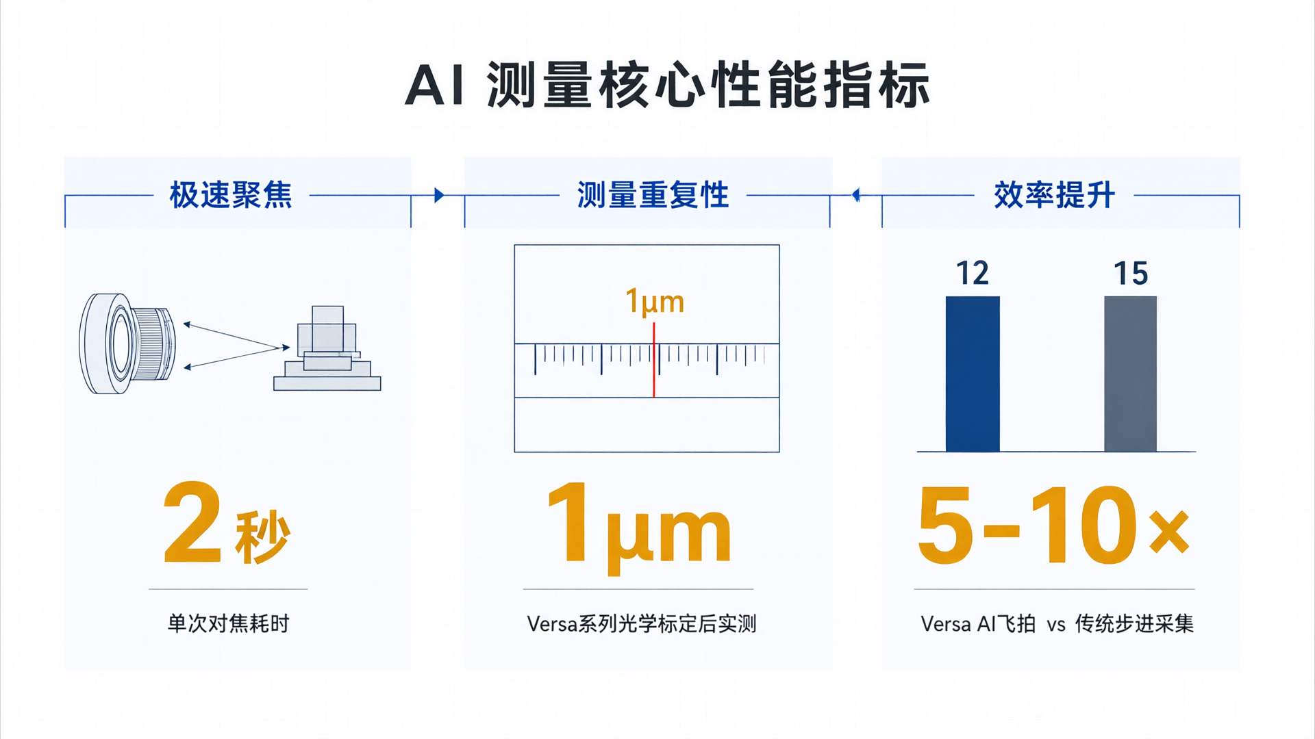

How does the Omni coordinate measuring machine ensure 1μm repeatability accuracy in semiconductor wafer inspection?
Posted2026-9-3
As semiconductor manufacturing advances to 3nm and beyond, tolerance windows for wafer-level inspection continue to narrow. The Maike ZhiCe Omni series CMM boasts a rated repeatability of 1 μm. This article analyzes its engineering implementation path across four subsystems: thermal field control, air-bearing motion systems, contact probe consistency, and software error compensation.
Semiconductor manufacturing is advancing to 3nm and below, causing tighter tolerance windows for wafer-level inspection. A single 12-inch wafer contains billions of chip structures; even micron-level geometric deviations can lead to significant yield loss. In this context, the repeatability accuracy of a Coordinate Measuring Machine (CMM)—defined as the consistency of multiple measurements of the same feature under identical conditions—determines whether process teams can trust the inspection data. The Maikozhi Ce Omni series CMM boasts a rated repeatability of 1μm, a figure achieved through the synchronized operation of tightly integrated engineering subsystems.
Thermal Field Control: The First Line of Defense Against Accuracy Drift
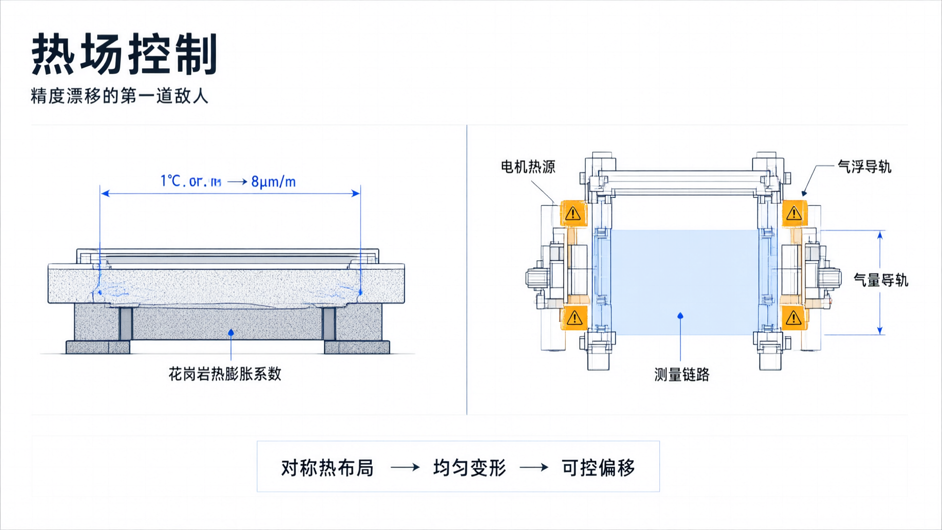
Structural components of coordinate measuring machines (CMMs) undergo slight deformation due to temperature fluctuations. Taking a granite worktable as an example, for every 1℃ change in temperature, the thermal expansion over a 1-meter length is approximately 8 μm—far exceeding the repeatability target of 1 μm. In semiconductor cleanrooms, although ambient temperatures are typically controlled within 20 ± 0.5℃, heat generated by the equipment itself (motors, drives, and friction pairs) still creates local temperature gradients.
The Omni series achieves convergence through structural design and environmental management. The bridge-type mobile structure separates the drive system from the measurement grating to minimize heat transfer from the motor to the measurement chain. A symmetrical thermal layout ensures uniform thermal deformation rather than unilateral offset. On the environmental side, customers must install a constant-temperature system that meets specified temperature fluctuation limits, effectively eliminating thermal drift at the installation stage.
Motion System: Integration of Air Floatation Guides and Drive Chain
Mechanical motion precision is built on repeatability. The Omni series uses all-air-bearing guides where moving parts do not contact the rails; instead, they are supported by a micrometer-scale air film generated by compressed air. This design eliminates stick-slip effects caused by sliding friction, ensuring continuous and smooth motion.
The drive system employs a DC servoless motor paired with a precision gearbox, achieving sub-micron encoder resolution. In typical semiconductor wafer inspection scenarios, the probe performs high-density matrix scanning across the worktable, requiring high motion frequencies and frequent acceleration/deceleration cycles. The zero-friction characteristic of the air-floating guide ensures consistent mechanical conditions for each positioning event, which is the fundamental prerequisite for maintaining repeatability.
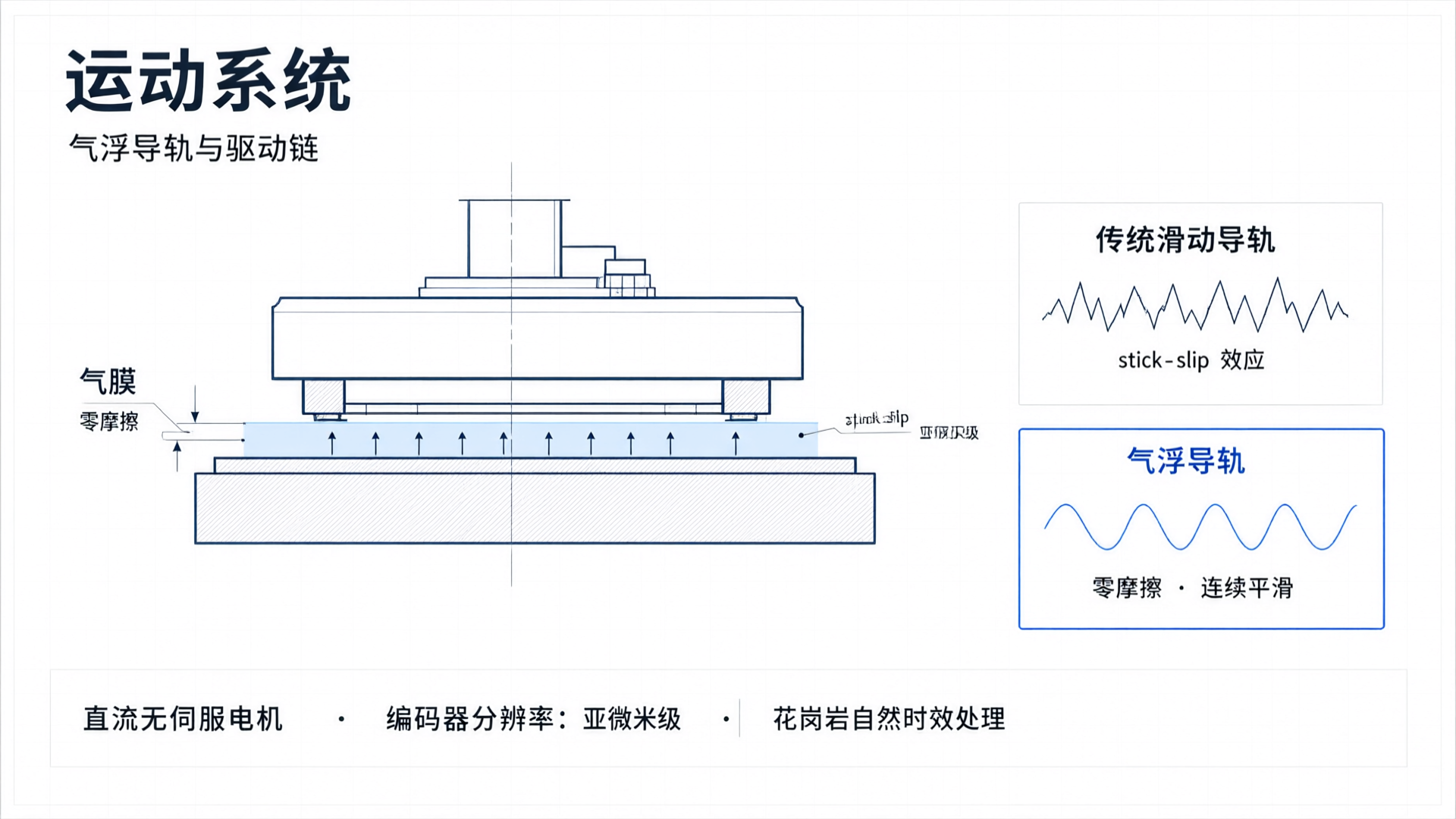
The granite platform undergoes natural aging to fully relieve internal stresses before precision machining, ensuring dimensional stability within controlled limits during long-term use. While this process extends lead time and increases costs, it significantly enhances the long-term accuracy stability.
Probe System: Trigger Consistency of Contact Probes
Coordinate measuring machines (CMMs) rely on contact probes: a ruby ball at the tip of the stylus touches the workpiece surface, and the moment the trigger signal is captured marks a coordinate sampling point. The repeatability of this process directly determines the consistency of measurement results.
The Omni series uses high-precision contact scanning probes for semiconductor wafer inspection. The core challenge lies in controlling probe overtravel—the tiny displacement between the probe tip contacting the workpiece and the trigger signal being recorded. This overtravel must remain consistent with every touch; any variation directly introduces measurement error. The Omni series achieves sub-micron trigger consistency through a rigid probe body, low-inertia stylus shaft, and sensor design that minimizes overtravel variation.
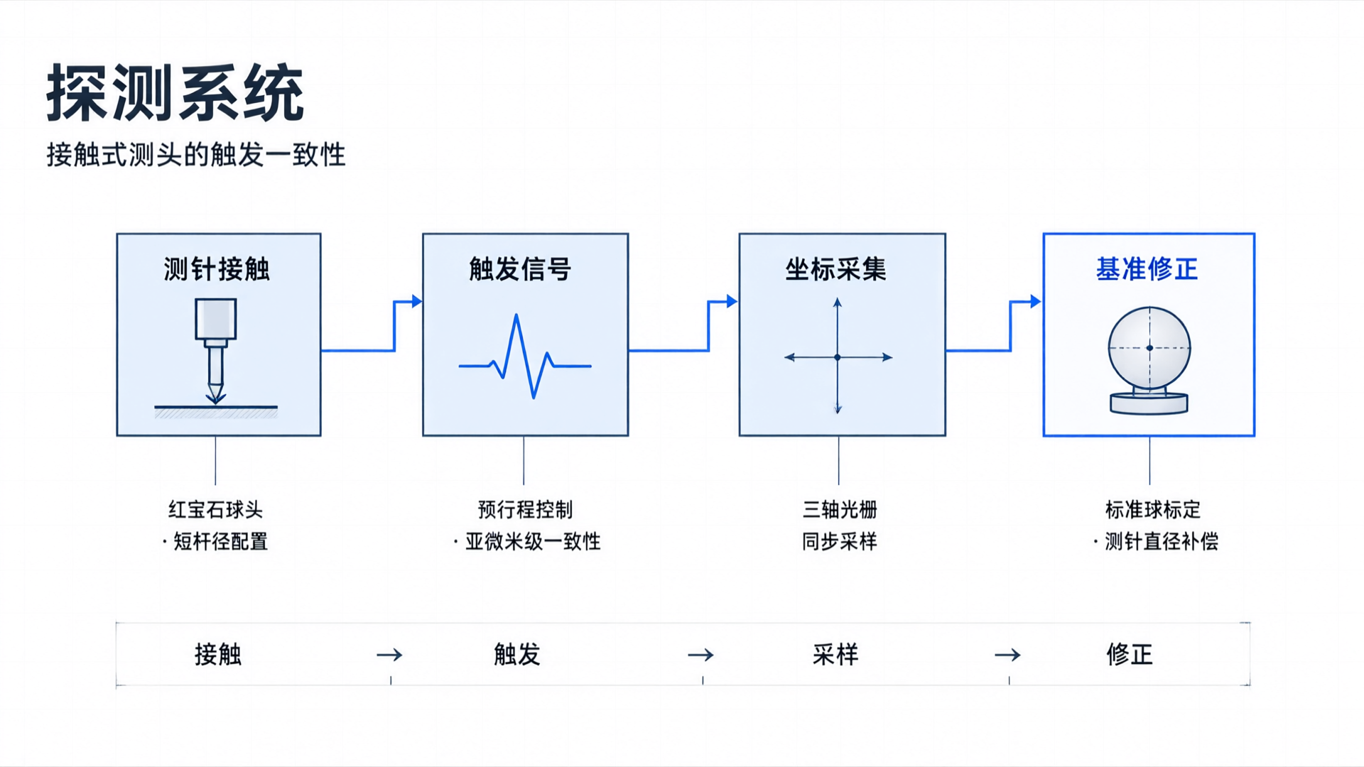
Probe selection directly affects repeatability. Longer probes with thinner stems experience greater bending deformation upon contact, increasing pre-travel variability. In semiconductor inspection, short-stem, small-ball-probe configurations are typically used to minimize mechanical variables while maintaining reachability. MicroCore AI measurement software performs probe calibration by collecting data from multiple points on a reference sphere to calculate the effective probe diameter and positional offset, which serve as correction values for subsequent measurements.
1μm repeatability is demonstrated here as: when a feature point is repeatedly touched, the variation in recorded coordinate values does not exceed 1μm. This result stems from the convergence of the probe's mechanical structure, the stylus's mechanical properties, and signal acquisition timing.
Software Compensation: Correct Systematic Errors
All precision mechanical systems have inherent systematic errors—linear deviations in guideways, scale line errors on grating rulers, and variations in probe pre-travel. These errors manifest as fixed offsets in single measurements; without correction, they directly accumulate into the measurement results.
MicroCore AI Measurement Software includes multiple error compensation features: after calibration with a laser interferometer, positioning, straightness, and angular errors are written to a compensation table for real-time correction during operation. Probe radius compensation is automatically calculated using calibrated sphere data to eliminate the impact of probe geometric deviations on measurement results. In high-volume semiconductor wafer inspection, the software also supports establishing mapping relationships between the measurement coordinate system and the wafer coordinate system, reducing human-induced deviations from fixturing and alignment.
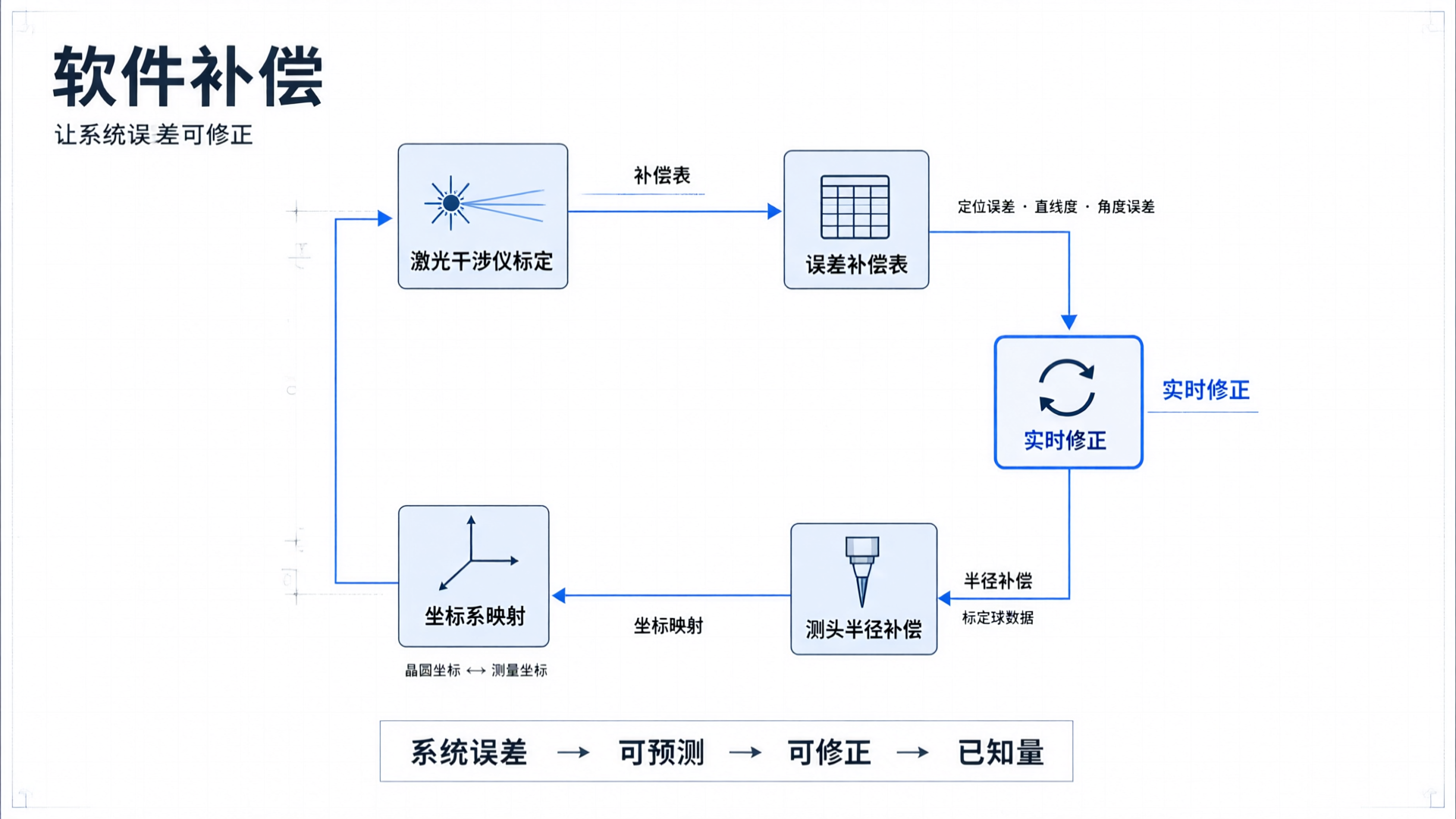
Software compensation doesn't alter the hardware's physical limits, but it transforms system errors from "uncontrollable drift" into "predictable, correctable known values."
System Integration Perspective
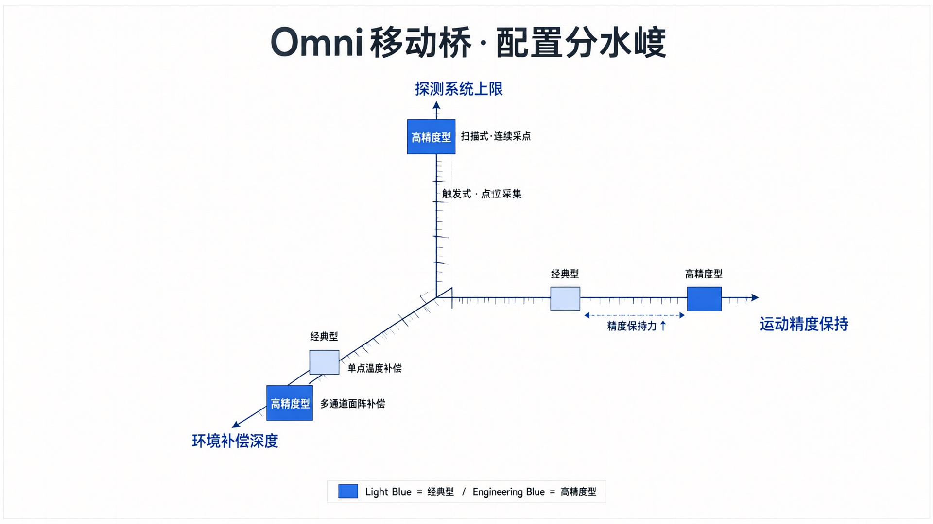
The 1μm repeatability is not the result of a single technology, but a system-level metric achieved when four subsystems—thermal management, motion control, signal detection, and software compensation—each converge to sufficiently small error margins. Semiconductor wafer inspection demands extreme data consistency: process engineers must confirm that differences between today's and yesterday's measurements stem from process variations, not equipment fluctuations.
The Omni series follows this engineering logic: air bearing structures eliminate friction randomness, thermally symmetric designs suppress thermal drift, signal chain stability ensures detection consistency, and software compensation cages system errors. All four elements are essential; any weakness causes overall repeatability to drop below the 1μm threshold.
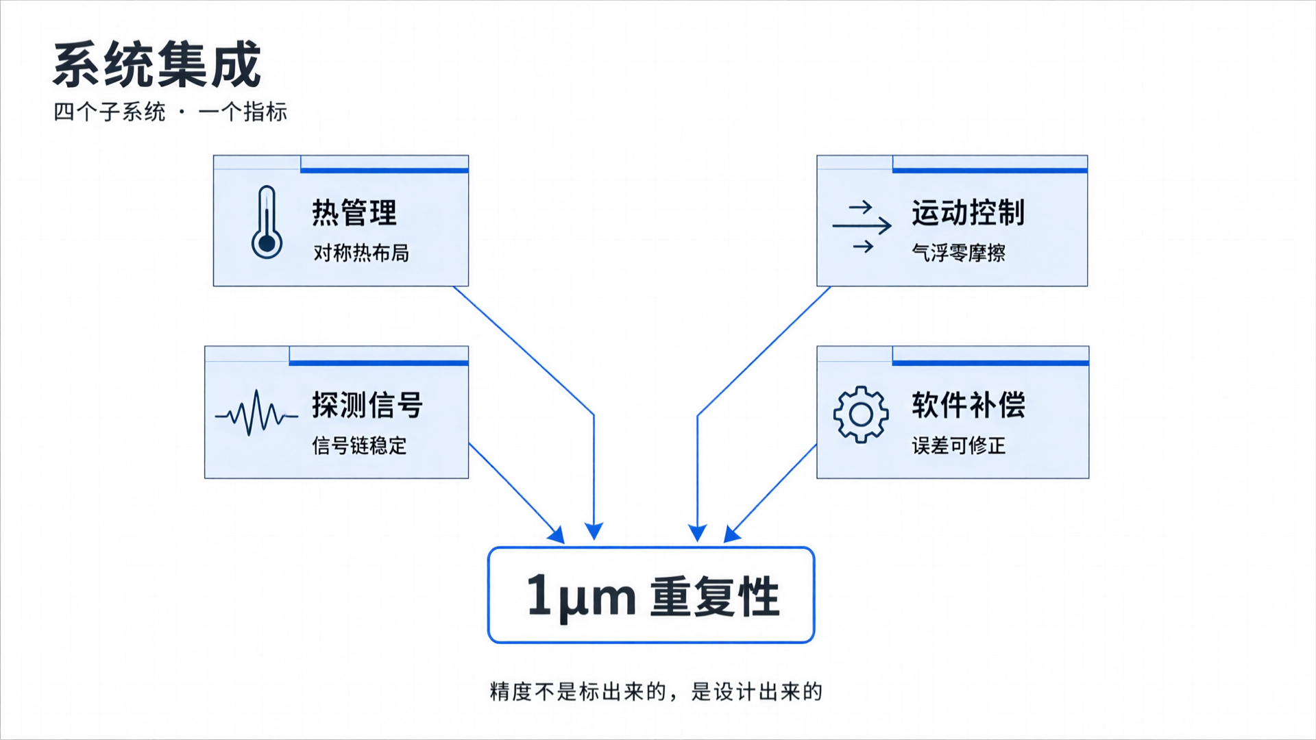
This is the fundamental difference between precision measurement equipment and general industrial equipment: accuracy isn't specified; it's designed in.